Products
Infinite Potentials of LTCC Applications
LTCC Materials provides the world with unique reliable products through its sophisticated LTCC technologies.
LTCC (Low Temperature Co-fired Ceramics) allows to use silver or copper conductors, which show lower electric resistivity compared with conductors used in other ceramics such as alumina. LTCC is a unique material the thermal, dielectric, optical and mechanical properties of which can be controlled by choosing glass and ceramic raw materials.
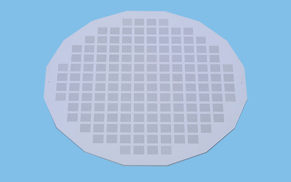
LTCC Materials provides reliable LTCC circuit substrate equipped with high-precision, high-density wiring.

LTCC: Ceramic substrate
Substrates for use in the wafer level CSP sector increasingly require high-density, high-precision pattern formation and flatness. It is necessary to increase the size of substrates in the field of semiconductor testing equipment, while high heat release, high brightness and high durability are required in the field of LED packages. LTCC Materials harnesses cuttingedge LTCC processing technology and 3D RF design technology to offer customers a variety of products that meet their needs with precision.
3-D RF Design
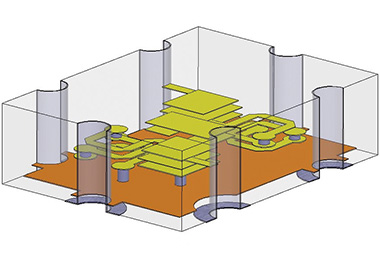
Using a circuit and electromagnetic field simulator, Ansoft Designer and HFSS, LTCC Materials provides circuit design and three-dimensional RF design for antennas, filters, RF module substrates and others.
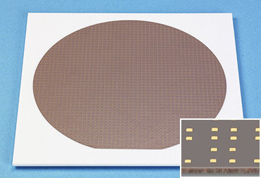
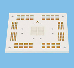
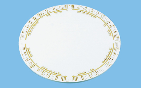
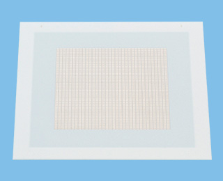
Interposer Substrate for Semiconductor Wafer Test
An LSI semiconductor wafer may have thousands of densely aligned bonding pads. LSI testing cannot be performed without a prober which physically expands the narrow pitch pads of the semiconductor to connect them to the tester. LTCC Materials, harnessing its cuttingedge LTCC process technology, has commercialized the interposer substrate used for the prober.
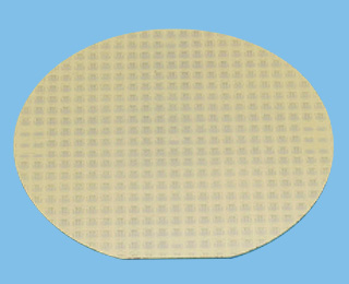
12 inch Interposer Substrate for Memory
(with Internal Power Supply and Ground)
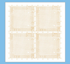
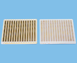
Interposer Substrate for Logic
(Multi Pin and DUT)
(50 Layers, Via Dia. : 50μm)
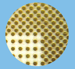
Min. Pad Pitch : Around 120μm
LTCC Applied Devices
LTCC Substrate for RF Application
- Dielectric Material for high frequency wave(εr :50)
- Self-developed material: YDM-500
(US PAT No.7781359)
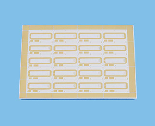
Substrate for RF Module
- Dimensions of product: 3.3×5.1×0.5mm
- Printed Resistor: 1Ω~10MΩ
LTCC Substrate Mounting High Frequency IC
- Mounting high frequency device
LED Substrate
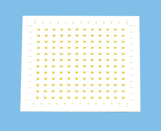
- High Reflection Material
- High Heat Dissipation
- Excellent mountability due to superior flatness
LED Substrate for Vehicle
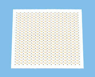
- For Mounting High-brightness LED
Super-thin LTCC CSP Substrate for LED
- Thickness: 0.075-0.150mm
LTCC Package for Arrayed LED Backlight
- Integrated Structure
- Uniform Light Emission better than Single Package
Other LTCC Product
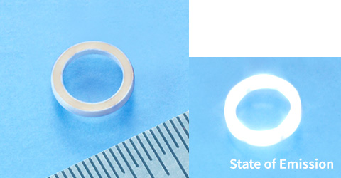
High Brightness/Ultraminiature LED RING LIGHT
A compact size, high-brightness, durable light source is required for miniature CCD cameras. LTCC Materials commercialized a high brightness /ultraminiature LED ring light to meets such requirements. This compact product, which equips plural LED devices, enables to be positioned right under a miniature CCD camera without optical fiber cables, and secure sufficient amount of light. It shows high durability by adopting our high temperature resistant LTCC substrate and special silicone resin sealing.
Application: Dental Instruments, Industrial/Medical Endoscope, Microscope etc.